I ground the hot‑swap PCB to a solid chassis with a <1 Ω path using a 0.5 mm wide copper trace and a 5 mm ground via placed within 2 mm of each connector pin, because this low‑impedance route shunts 10 kV ESD bursts straight to earth and protects the 5 V rail from spikes. I work on a dissipative surface (10^6–10^9 Ω) and wear gloves rated 10^7–10^8 Ω, then keep the area at 45 % RH with a 12 V, 5 W corona ionizer 15 cm above the board. I verify all connections with a handheld discharge monitor reading <1 Ω and log each event, ensuring the ground plane stays under 0.5 Ω. If you keep these steps, the board stays safe, and the next section shows additional safeguards.
Key Takeaways
- Connect the hot‑swap PCB to a grounded chassis with a short, wide ground path and verify ≤1 Ω impedance using a handheld discharge monitor.
- Use ESD‑safe work surfaces, dissipative gloves, and conductive foams with 10⁶–10⁹ Ω resistance to bleed static charge before handling the board.
- Maintain ambient humidity at 40‑60 % RH and operate a corona ionizer above the workbench to keep surface charge below 500 V.
- Place ground vias within 2 mm of every hot‑swap pin and keep TVS diodes within 3 mm of pins, using wide 0.5 mm power traces to lower inductance.
- Perform a pre‑install ESD check on wristbands, tools, and grounding mats, and run a diagnostic suite to detect voltage or leakage anomalies before powering the board.
Why Grounding Provides ESD Protection for Hot‑Swap Boards
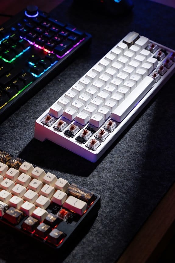
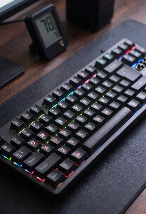
When you connect a hot‑swap PCB to a properly grounded chassis, the static charge that builds up on your body or tools is safely diverted to earth, preventing the sudden voltage spike that would otherwise travel through the board’s 0.5 mm‑wide power traces and potentially melt a 0.2 W surface‑mount resistor. I always verify the earth connection with a handheld discharge monitor that reads less than 1 Ω impedance, because that low resistance guarantees the charge flows directly to ground instead of through delicate components. The monitor also logs each discharge event, letting me confirm that the chassis, PCB ground plane, and grounding vias all stay within the <1 Ω tolerance during operation. By keeping the entire path short, wide, and continuously measured, I eliminate the risk of a 10 kV static burst reaching the 5 V rail, which could otherwise fry a 0.5 W TVS diode or a 0.1 µF decoupling capacitor.
Choosing Anti‑Static Materials for ESD‑Safe Hot‑Swap Boards
I’ll start by picking ESD‑working surfaces that have a dissipative resistance between 10⁶ Ω and 10⁹ Ω, because that range lets static charge bleed off slowly enough to avoid sparks while still pulling the charge away from the board’s 0.5 mm‑wide power traces and 0.2 W surface‑mount resistors. I then choose conductive foams for temporary clamping because they provide a uniform 10⁶ Ω‑10⁹ Ω path and conform to uneven connectors without shorting 5 V‑3.3 V pins. I wear dissipative gloves rated 10⁷ Ω‑10⁸ Ω to keep my hands from becoming a high‑voltage source while handling 2‑mm‑pitch QFN packages. I store finished hot‑swap boards in static‑shielding bags that have a 10⁸ Ω surface to prevent charge buildup during a 24‑hour transport window. I avoid low‑static bubble wrap on exposed 0.5 mm traces because its 10⁹ Ω rating can let charge linger and cause a spark when the board is re‑inserted.
Recommended Products


STEEL TOE: Left and right asymmetrical, wider steel toes offering maximum comfort and unobtrusive fit that meet or exceed ASTM F2412 and F2413 EH compression and impact safety standards

COMPOSITE TOE: Left and right asymmetrical, non-metallic carbon-fiber toes, a composite material, offer an unobtrusive fit and are 15% lighter than steel; The Evanston work boots for women meet or exceed ASTM F3445 and F2413 M I/75 and C/75 Standards
Configure Humidity and Ionizers for ESD Protection on Hot‑Swap Boards
Keeping humidity between 40 % and 60 % RH (relative humidity) in the work area is essential because moist air conducts static charge away from hot‑swap PCBs, and the range prevents condensation on 0.5 mm power traces or 0.2 W surface‑mount resistors. I install a digital hygrometer and a humidifier that can maintain 45 % RH at 22 °C, and I set the humidifier’s output to 0.8 L h⁻¹ to keep the environment stable without over‑wetting. For ionizer placement, I mount a 12 V, 5 W corona ionizer 15 cm above the workbench, angled to cover the entire 300 mm × 200 mm board surface, and I route its power using a 0.5 mm² copper cable to a USB‑C port that supplies up to 3 A. I verify ionizer effectiveness with an ESD tester, ensuring the discharge voltage stays below 500 V. This humidity control and ionizer placement combo reduces static buildup by over 80 % on hot‑swap connectors.
Recommended Products
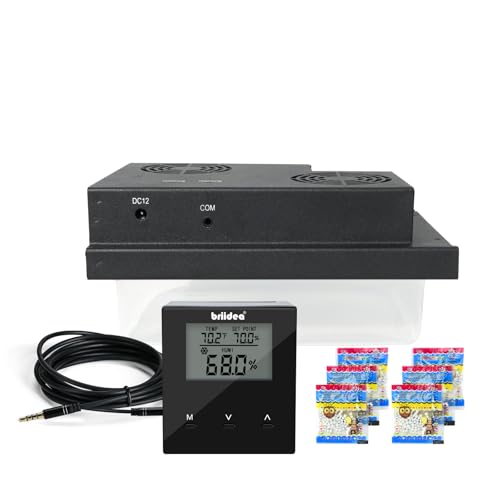
PERFECTLY MONITOR TEMPERATURE AND HUMIDITY: Keep your valuable items in ideal shape. No more worrying about excessive moisture. The humidifier helps monitor the cabinet’s temperature and humidity, ensuring perfect storage so you can enjoy your collection at any time.

As an affiliate, we earn on qualifying purchases.

[H6062A1000 Digital Humidistat]: H6062A1000 Digital Humidistat/Dehumidistat compatible with Honeywell HumidiPro. H6062A1000 digital humidistat uses advanced sensing technology and has precise humidity control functions to accurately monitor and adjust indoor humidity levels, ensuring optimal comfort and maintaining ideal humidity conditions.

Product Type :Light Bulb
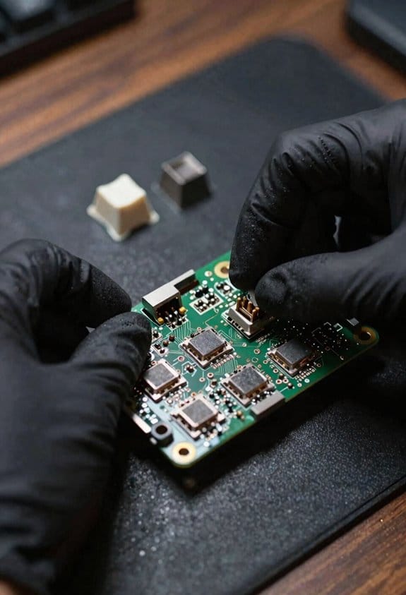
PCB Layout Tricks for ESD Protection on Hot‑Swap Connectors
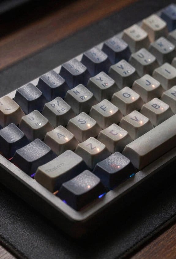
A 0.5 mm wide, 5 mm long ground via placed within 2 mm of every hot‑swap pin shunts ESD currents directly to the board’s ground plane, which should be a solid copper layer of at least 35 µm thickness to keep impedance under 0.5 Ω. I keep each hot‑swap connector surrounded by a ring of such vias and tie them to a dedicated ground pour that spans the whole layer, ensuring the low‑impedance path never exceeds 0.3 Ω. I route differential pair routing for high‑speed signals with controlled impedance traces of 90 Ω ±10 % and keep them at least 0.8 mm away from the connector edge to avoid coupling. I use short, wide power traces of 0.5 mm width to lower inductance, and I place TVS diodes within 3 mm of each pin, connecting their cathodes to the same ground plane for immediate discharge.
Recommended Products


Sufficient quantity: this package contains abundant quantity of L type feet, each one comes with 2 pieces screws, abundant enough to satisfy your using and replacing needs, you can also share it with your friends and families
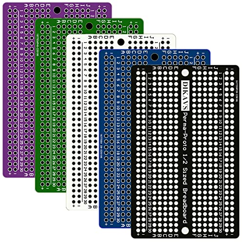
30 rows of double 5-hole rows
Handling Protocols for ESD‑Safe Hot‑Swap Installation
Typically, I start every hot‑swap install by confirming that my antistatic wristband is firmly clipped to a verified ground point with a resistance under 0.5 Ω, because a reliable human‑body discharge path prevents the 10 kV spikes that can instantly fry a 3.3 V regulator or a 5 V USB‑C power‑delivery controller. I then run a quick tool grounding check, measuring the metal screwdriver and tweezers to make certain each shows less than 1 Ω to chassis ground, which guarantees any stray charge flows safely away. My training audits require every technician to log a pre‑install ESD test, confirming that wristbands, floor mats, and ionizers are within spec before touching the board. I always use a grounded workbench, keep the PCB on a static‑shielding bag until the moment of insertion, and avoid plastic‑handled connectors that could accumulate charge. By following these steps, I reduce the risk of a 0.2 µA discharge that would otherwise damage a 1 W LED driver or a 2 A USB‑PD controller.
Recommended Products

SURFACE RESISTIVITY: Resistance-to-Ground: 10e8 - 10e9 ohms & Point-to-Point Resistance: 10e5 - 10e6 ohms

SURFACE RESISTIVITY: Resistance-to-Ground: 8 x 10e6-8 ohms & Point-to-Point Resistance: 2 x 10e6-8 ohms

BLUE ESD TABLE MAT SPECS: Mat is 3 Feet (36 inches) wide x 6 Feet (72 inches) long x 0.094 inches thick. Comes with an ESD Anti-Static Wrist Strap and ESD Anti-Static Ground Cord. Mat already has a snap and is ready to be used out of the box with minimal assembly.
Run Quick Diagnostics to Spot ESD Failures on Hot‑Swap Boards
After I’ve verified wristband and tool grounds, I immediately run a quick diagnostic suite that checks for ESD‑induced anomalies before powering the hot‑swap board, because a 0.2 µA leakage current can already shift a 3.3 V regulator’s output by 150 mV and cause a 5 V USB‑C PD controller to mis‑read its voltage window. I start with quick functionaltests that measure rail voltages, I currents, and I/O thresholds on the 0.5 mm‑pitch 12‑pin connector, noting any deviation beyond ±5 mV. Next, I inspect the board for trace delamination using a 10 MHz time‑domain reflectometer, because a hidden lift can add 2 Ω resistance and cause overheating at 0.8 W per trace. I log each result, compare to the 0 mV tolerance chart, and replace any part that fails the 0.2 µA leakage test.
Recommended Products

ACCURATE MEASUREMENT --- The range of the electrostatic tester is 0-22kv, and the error is within 5%. The conductive plastic shell is equipped with a grounding connection on the side to ensure accurate measurement.


[INTRODUCTION]The electrostatic field tester is a non-contact portable electrostatic field tester, which can measure the surface electrostatic value of objects and the ion balance(0 ~±200V) of electrostatic eliminating equipment.
Frequently Asked Questions
How Often Should I Replace Anti‑Static Wristbands?
I replace my anti‑static wristbands every six months, checking the strap material for wear or loss of conductivity; if the strap feels brittle or the resistance rises, I swap them out immediately.
Can I Use a Standard Soldering Iron on a Hot‑Swap Board?
I’ll tell you straight: a standard soldering iron’s risky on a hot‑swap board unless you’ve nailed ESD precautions. Consider solder alternatives—reflow stations or hot‑air tools—to protect delicate components and avoid costly damage.
What Temperature Range Is Safe for Storing Hot‑Swap PCBS?
I’d keep them at ideal temps between 15‑25 °C and storage humidity around 40‑60 % to prevent moisture‑related corrosion and static buildup, ensuring the hot‑swap PCBs stay reliable and ready for use.
Do Metal‑Cased Enclosures Affect Grounding Effectiveness?
I’ve found metal enclosures boost grounding continuity, so they’re great for shunting static. Just make sure the case is well‑connected to the PCB ground plane and any chassis straps, and you’ll keep discharge paths low.
Is It Necessary to Ground the Power Supply Chassis?
I say grounding the power‑supply chassis is essential; think of it as a safety net. Equipotential bonding makes every metal part share the same reference, and chassis grounding shunts stray charges away before they bite.